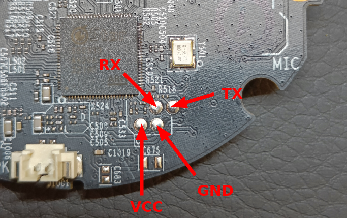
UART Interface Discovery
During the Hardware Analysis chapter, apart from the identified components, a set of four unpopulated pads located on the top side of the main PCB stood out as a likely debug interface.
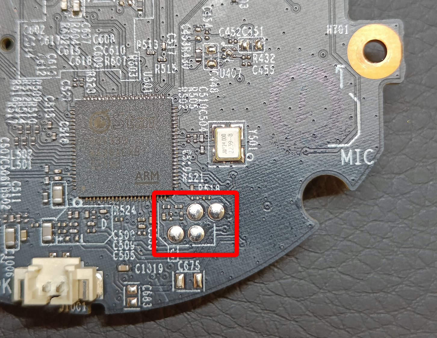
Based on their layout and proximity to the SoC, these pads were suspected to be a UART serial interface. This was also confirmed when viewing the “Getting UART” video documented during the OSINT phase. Therefore, the goal of this phase was to validate the serial communication by firstly identifying the UART port pinout and observing its output.
Identifying the UART pads
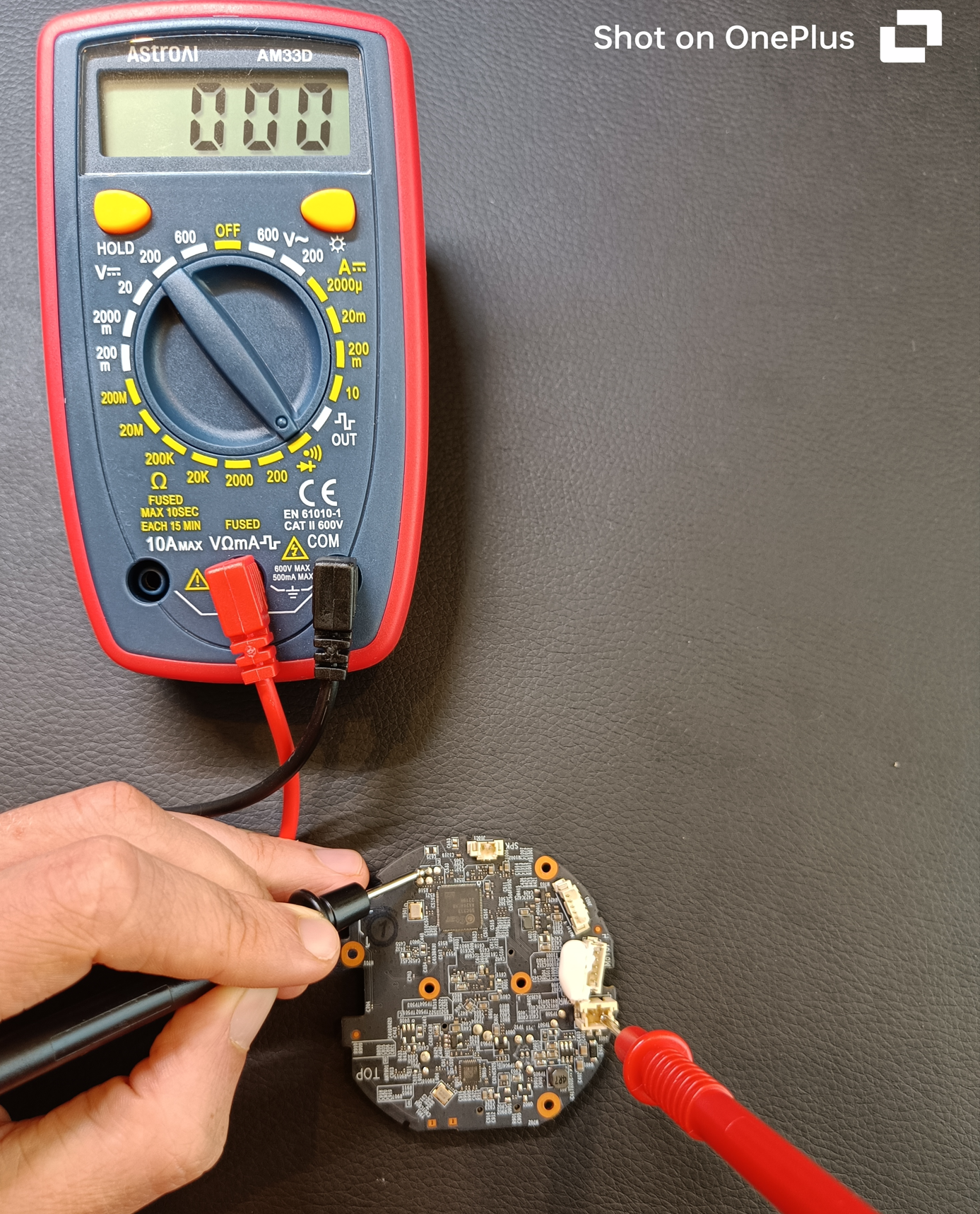
The first step was to identify the ground (GND) pads. For this, a continuity test was performed using a multimeter between each of the four pads and known ground reference points on the PCB, as seen in the image below.
With the ground pad identified, the target was powered on and the voltage of the remaining three pads was measured relative to GND. Typical UART characteristics were used to identify the remaining pads:
| Pad | Expected Behavior | Observed Characteristics |
|---|---|---|
| VCC | Power rail | Steady ~3.3V |
| TX | Data output | Fluctuating voltage due to data transmission |
| RX | Data input | Steady ~3.3V (idle logic level high) |
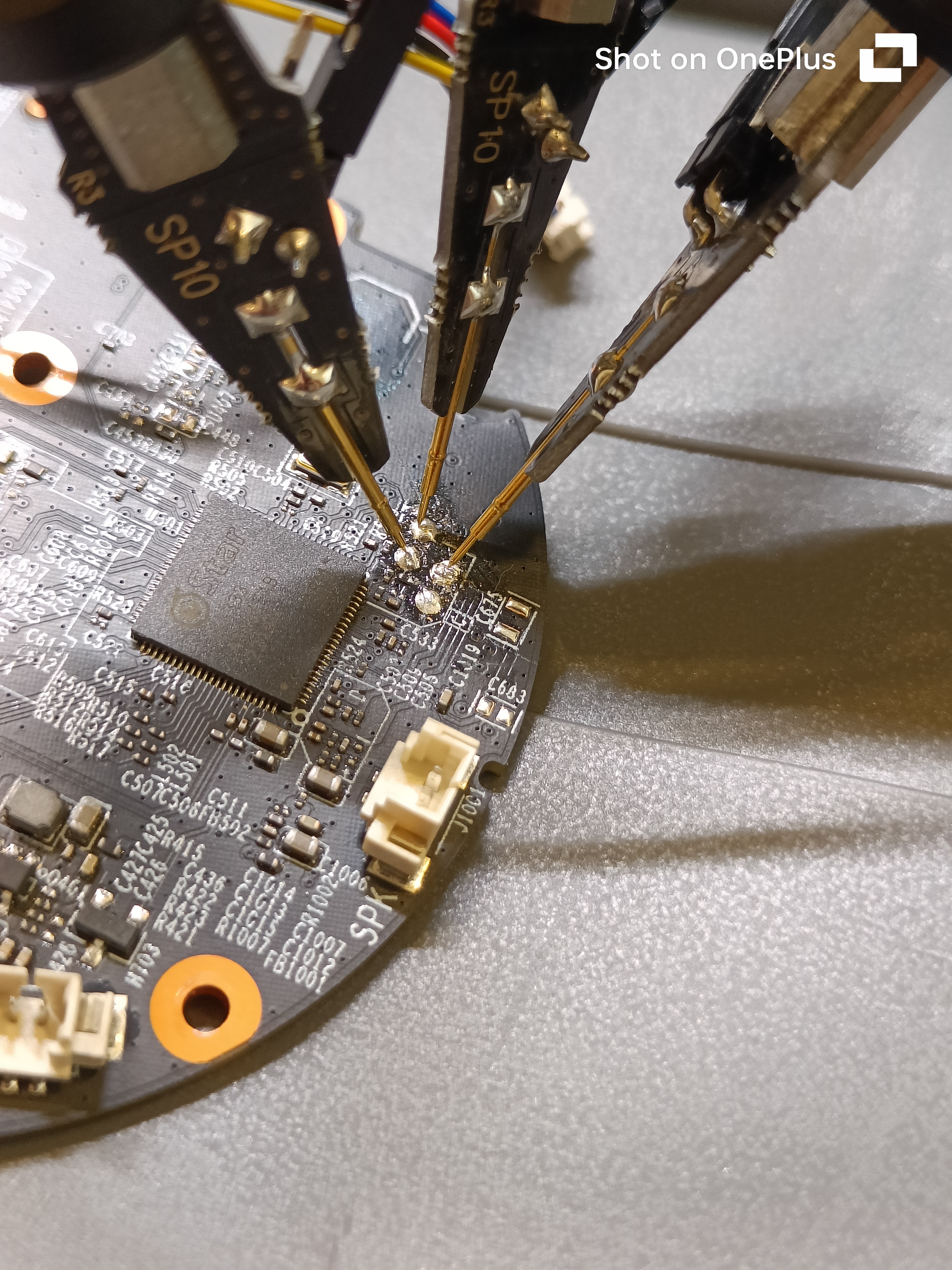
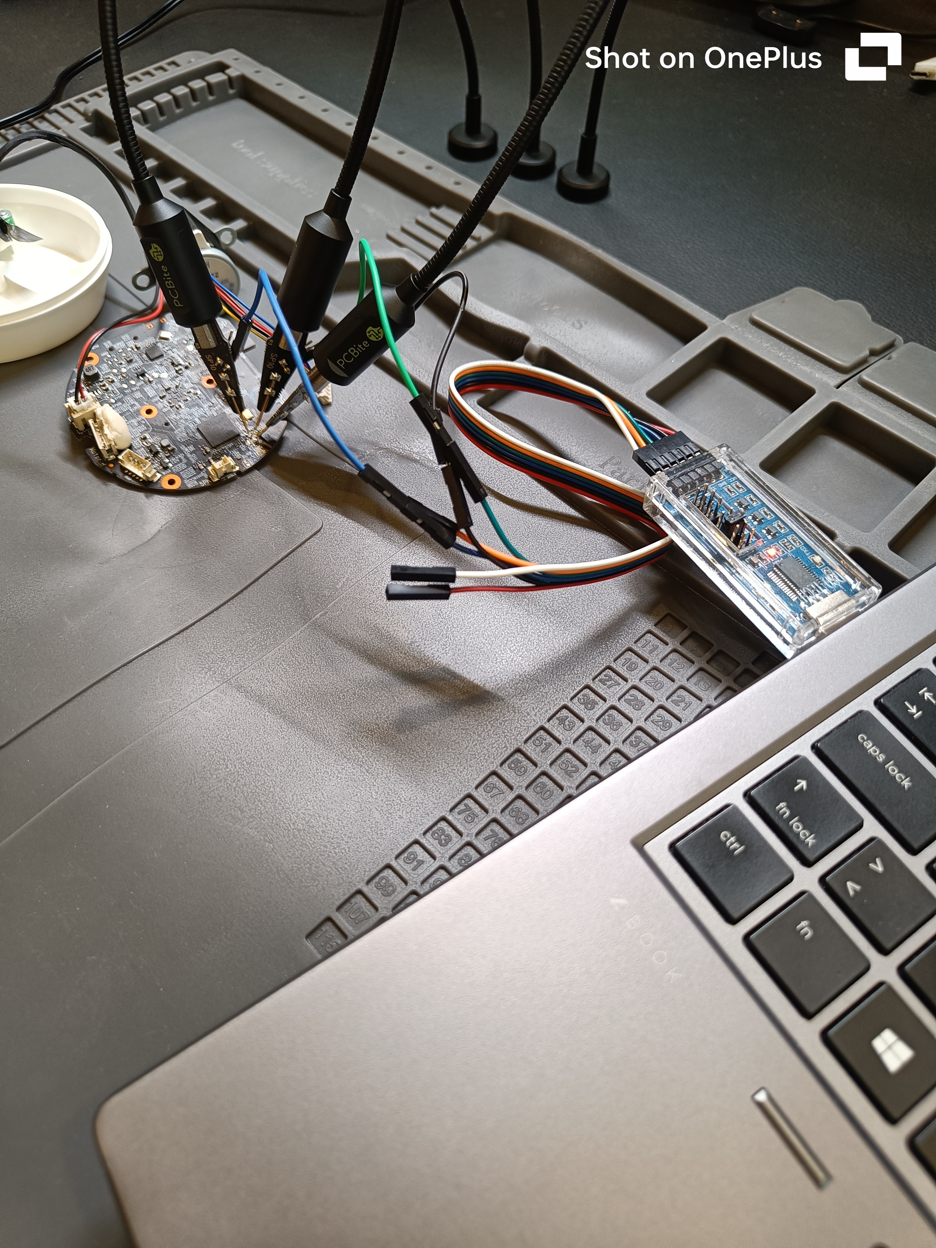
Of the remaining pads, TX was the first to be identified due to its fluctuating nature on device boot. However, since VCC and RX possessed the same voltage level, a USB-to-TTL adapter was used in order to determine RX, by connecting the TX pin of the adapter to each of these two pads and verifying which allowed for communication between the Kali station and the target, as seen in the images below.
Finally, it was possible to determine the UART pads, as seen in the image below: